
App Note: Fast Fiber-to-Chip Peak Search for PIC Wafer-Level Testing
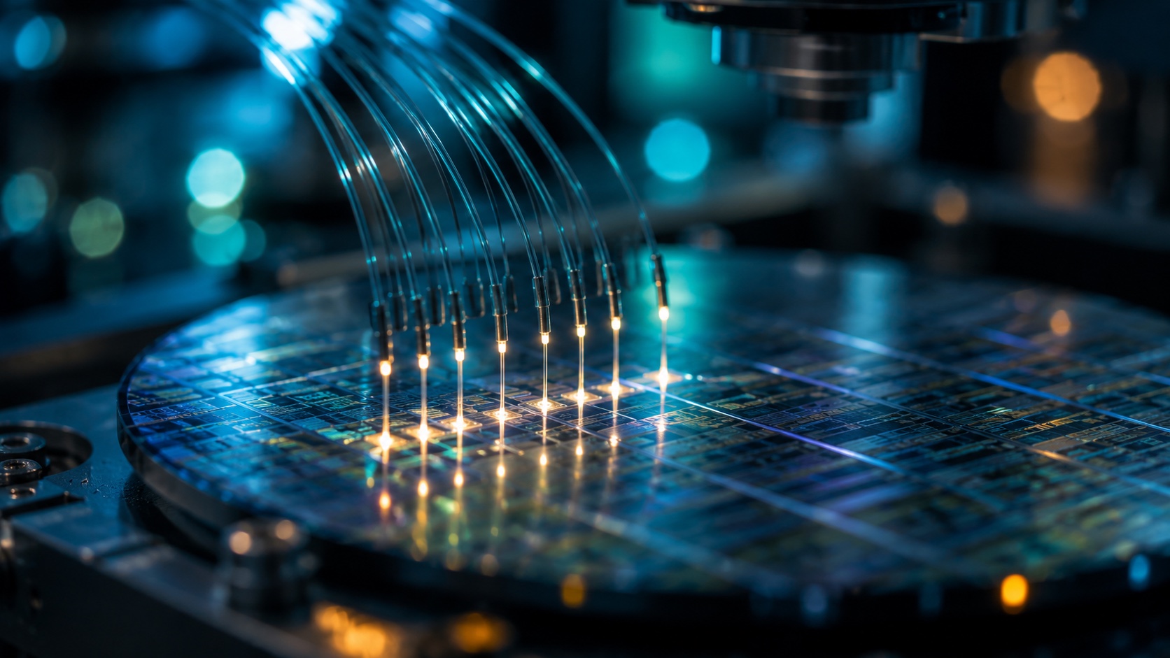
Silicon photonics and co-packaged optics are scaling fast, but photonic chips must be optically tested at wafer level — and every test site requires active fiber-to-chip alignment within a ±0.5–1 µm 1-dB tolerance. Alignment speed directly determines wafer test throughput.
Nahshon has completed the Traditional Chinese edition of the piezosystem jena application note “Fast Fiber-to-Chip Peak Search for PIC Wafer-Level Testing”: dual TRITOR 100 SG stages with NV 40/3 CLE controllers achieve a position-referenced coupling map in a ~0.8 s open-loop spiral scan, for ~5 s total alignment per site.
Contact us for the full document — and see the live demo at Booth P821, Hall 2, Aug 19–22.