
App Note: Fast Fiber-to-Chip Peak Search for PIC Wafer-Level Testing
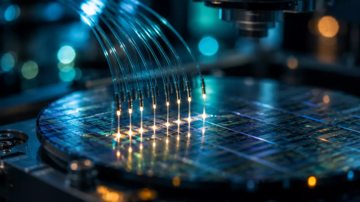
Silicon photonics and co-packaged optics are scaling fast, but photonic chips must be optically tested at wafer level — and every test site requires active fiber-to-chip alignment within a ±0.5–1 µm 1-dB tolerance. Alignment speed directly determines wafer test throughput.
Nahshon has completed the Traditional Chinese edition of the piezosystem jena application note “Fast Fiber-to-Chip Peak Search for PIC Wafer-Level Testing”: dual TRITOR 100 SG stages with NV 40/3 CLE controllers achieve a position-referenced coupling map in a ~0.8 s open-loop spiral scan, for ~5 s total alignment per site.
Contact us for the full document — and see the live demo at Booth P821, Hall 2, Aug 19–22.
FAQ
光纖對晶片對位為什麼需要主動尋峰?
晶片耦合器的 1-dB 對位容差只有 ±0.5–1 µm。機械定位或機器視覺可用於初步對位,但若要直接最佳化實際光耦合效率,可利用光功率作為回授訊號,透過主動掃描尋找峰值位置。
一個測試點的對位要花多久?
單次螺旋掃描約 0.8 秒,含粗定位與精掃的每站總對位時間約 5 秒。架構是兩座 TRITOR 100 SG 三軸壓電平台,各由一台 NV 40/3 CLE 控制器驅動。
對位慢一秒對產能影響有多大?
每個測試點多花 1 秒,整片晶圓就多出約 1 小時的機台時間。這也是光子晶圓級測試把對位速度當成首要指標的原因。