
Piezo Nanopositioning in Semiconductor Lithography
Photolithography is a key process in the manufacturing of semiconductors.
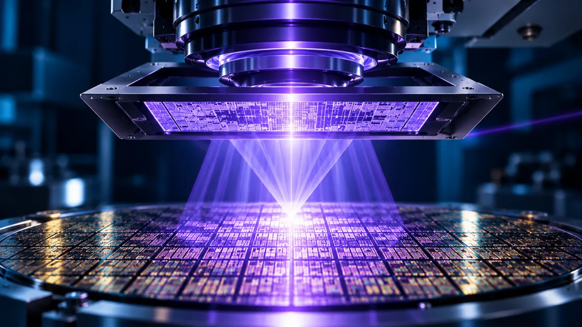
The process begins with a photomask of electronic circuits. This photomask is essentially a template for the chips that will be produced on the silicon wafer. UV or EUV light is then shown through the mask and a series of lenses onto the wafer, resulting in the patterning of the silicon. This process is repeated until the silicon is completely patterned on all layers. The patterned wafer can then enter the next step of production. This patterning of the silicon by the process of photolithography is a vital step in the very delicate and tedious process of wafer chip production.
The semiconductor lithography process is extremely precise and typically includes piezo positioning components.
As with every step of semiconductor manufacturing, the positioning of the wafer during photolithography is extremely important. If the wafer is out of position, the silicon will not be patterned correctly. For this reason, piezoelectric stages are commonly used to position the wafers during this step of production. Providing up to 5 axes of motion with nanometer and microradian precision, piezo stages provide a perfect solution for this highly technical procedure.
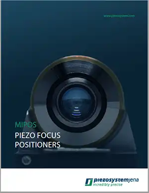
Equally important during the photolithography process is the positioning of the lenses/objectives as they are responsible for focusing the light on the wafer. piezosystem jena has stages and microscope objective positioners (MIPOS) to aid in exactly this task.
Whitepaper: Beyond Microscopy – MIPOS in Industry Applications
FAQ
微影製程裡壓電平台負責什麼?
負責晶圓定位。晶圓一旦偏離位置,矽材上的圖案就無法正確成形,而壓電平台可提供最多 5 軸運動、具備奈米級與微弧度級精度,適合這種高度精密的製程。
除了晶圓,還有哪個環節需要精密定位?
透鏡與物鏡——它們負責把光聚焦到晶圓上,定位同樣關鍵。piezosystem jena 的定位平台與顯微物鏡定位器 MIPOS 就是為這項任務設計的。
光學微影的圖案是怎麼轉移到晶圓上的?
製程從承載電子電路圖形的光罩開始,讓 UV 或 EUV 光穿過光罩與一系列透鏡照射晶圓,在矽晶圓上形成圖案,反覆進行直到所有層都完成圖形化。圖形化後的晶圓才能進入下一道製程。