
Optical Z-Scanning Using MIPOS with Minimal Lateral Runout

1. Application Background
Surface flatness inspection of semiconductor wafers and large-area flat-panel display (FPD) substrates is a critical step in process control for advanced packaging and display manufacturing. Local height variations, warpage, and step heights at the nanometer scale directly affect downstream process yield — for example, the planarity tolerance required for hybrid bonding and die-to-wafer placement in advanced packaging, or the focus-margin budget in FPD lithography.
No surface is perfect. Local height variations, warpage, and steps at the nanometre scale are common imperfections one has to deal with during semiconductor manufacturing. In order to manufacture structures with long-term process stability, it is therefore often necessary—as pitch sizes decrease—to measure the imperfections of each individual substrate so that they can be corrected in subsequent process steps. When smaller and smaller structures are desired, processes like hybrid bonding, die-to-wafer placement in advanced packaging, or the FPD lithography require a good measurement method to characterize the surface.
Surface flatness measurements are typically performed with interferometric or confocal microscopy, in which a precision Z-stage scans the objective lens through a focus or fringe-scan range while the optical system records surface topography. The Z-axis stage therefore directly determines the achievable depth-of-field coverage of the tool. It is even more critical that any horizontal movement or rotation of the lens during the z-scan results in a position dependent shift in the image of the substrate area being imaged—thereby creating topography artifacts that are indistinguishable from true surface features. It is therefore desired to have a perfect Z-line motion of the actuator moving the lens system.
2. Positioning Requirements
For this OEM inspection platform, five parameters were specified as hard limits:
| Parameter | Specification |
|---|---|
| Z-axis travel | 500 μm |
| Z-axis positioning resolution | ≤ 5 nm |
| Tip/tilt (XY), full Z-stroke | ≤ 5 μrad |
| Horizontal (XY) runout at substrate plane, full Z-stroke | ≤ 50 nm |
| Lateral runout, standard MIPOS (reference) | ≤ 350 nm |
The 500 μm Z stroke is dictated by the total thickness variation and warpage of the substrates under inspection. The 5 nm Z resolution is required so that the positioner does not contribute quantization artefacts above the noise floor of the optical measurement. The 50 nm horizontal runout limit is set by the optical pixel size of the inspection sensor and the customer’s measurement uncertainty budget; above this threshold, the horizontal wander of the imaged region during a Z scan would dominate the height map noise.
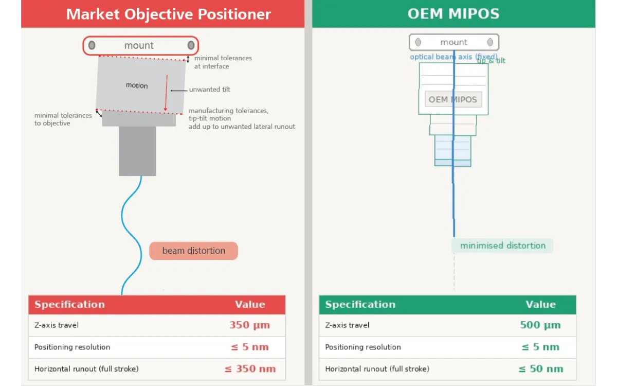
For reference, the horizontal runout of a standard MIPOS 500 over the same Z-stroke is in the range of 350 nm — fully adequate for microscopy autofocus, but approximately 7 times above what this inspection application can tolerate.
3. OEM-specific Optimizations
To meet the 50 nm horizontal runout target while preserving the full 500 μm Z stroke and ≤ 5 nm Z resolution, piezosystem jena implemented targeted improvements in two areas.
3.1 Mechanical design
The monolithic flexure guidance of the standard MIPOS 500 was redesigned using finite-element analysis with parasitic-motion minimisation as the primary goal. Modifications addressed the symmetry and stiffness ratio of the parallelogram flexure pairs, the rotational stiffness about the parasitic (off-axis) axes, and the balance of the moving mass to reduce off-axis coupling between Z-translation and X/Y-excursion. The intent is to drive the dominant horizontal and rotational error modes well below the customer’s measurement budget. Additionally, stable parameters were chosen to accommodate for machining tolerances of the solid-state joints.
3.2 Manufacturing process
Long partnership with external suppliers led to mutual understanding where machining tolerances could be improved by applying new processes. This leads to stricter geometric tolerances on the wire-EDM flexure features, better pairing-and-matching piezo stack selection to minimize hysteresis asymmetry, and a controlled assembly procedure with in-process metrology to ensure consistent axial preload and minimal residual horizontal bias. 100% control verified high yields and process stability under standard manufacturing conditions, confirming a robust design was developed.
4. Qualification Methodology
Each OEM unit is qualified before shipment against two independent interferometric metrology references:
- Michelson interferometer (Z-axis). A stabilised Michelson interferometer with a HeNe reference laser measures commanded-vs-actual Z displacement across the full 500 μm stroke. This verifies linearity, repeatability, and resolution at the sub-nanometer level, traceable to the laser wavelength.
- White-light (low-coherence) interferometer (horizontal runout). A calibrated flat substrate is imaged through the MIPOS-mounted objective. Surface features are tracked through the full Z-stroke, and the substrate-plane horizontal position is extracted at multiple Z-setpoints. The maximum horizontal excursion across the stroke is reported as the XY-runout figure. White-light interferometry is used in preference to monochromatic fringe analysis because the broadband coherence envelope removes 2π phase ambiguity over the long Z-range and provides direct topographic context of the reference surface.
The measured qualification record is delivered with the unit.
5. Summary
The OEM MIPOS 500 variant developed for this inspection platform delivers a combination of 500 μm Z-stroke, 5 nm Z-resolution, tip/tilt of 5 μrad and ≤ 50 nm horizontal runout at the substrate plane — a specification not available in the standard catalogue product. The improvement is achieved through coordinated changes in mechanical design and manufacturing process, qualified against traceable Michelson and white-light interferometric references. The result is a Z-axis positioner that customers can integrate directly into equipment used to test the flatness of wafers and flat-panel displays, offering predictable, documented performance.
FAQ
MIPOS 的橫向偏擺能壓到多小?
這套 OEM 版 MIPOS 500 在全 500 µm Z 行程下做到基板平面橫向偏擺 ≤50 nm,同時維持 ≤5 nm 的 Z 解析度與 ≤5 µrad 的繞 X/Y 軸傾斜角。作為對照,標準 MIPOS 500 在相同 Z 行程下的橫向偏擺約 350 nm——對顯微鏡自動對焦完全足夠,但約為此檢測應用可容忍值的 7 倍。
50 nm 這個門檻是怎麼定出來的?
由檢測感測器的光學像素尺寸,以及客戶允許的量測不確定度範圍設定。超過這個門檻後,Z 掃描期間成像區域的橫向位移會開始主導高度圖的雜訊,並可能產生難以與真實表面特徵區分的假影。
偏擺有沒有實測驗證?怎麼量?
每台出貨前都以兩套獨立的干涉基準驗證:以穩頻 HeNe 雷射為基準的邁克生干涉儀量全行程 Z 位移,白光(低同調)干涉儀量橫向偏擺。選白光而非單色條紋分析,是因為寬頻同調包絡能在長 Z 範圍內消除 2π 相位模糊。每台產品均隨附實測驗證紀錄。