
Piezo Positioning Solutions for Semiconductor Wafer Inspection
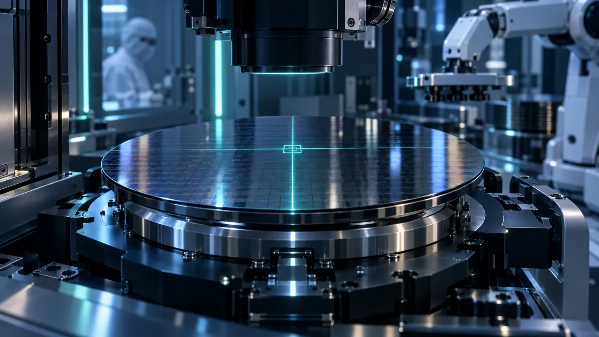
During the semiconductor wafer lithography, inspection, and dicing processes, the exact positioning of the wafer is critical. Today’s roadmap consists of features down to single digit nanometers, meaning the positioning system needed to create these features must have even smaller resolutions. Piezo actuators serve as the perfect tools to create this extremely precise and accurate positioning.
Piezo actuators are used as an OEM component in a variety of semiconductor production machines. Piezo stages move the wafer on demand in sub-nanometer steps per alignment marks or manual adjustment by an operator.
Piezo Solutions for Semiconductor Manufacturing Applications
Piezo stages from piezosystem jena utilize a FEM optimized flex hinge design to ensure the highest performance during this wafer positioning process. The benefits include:
- The solid-state design allows for no mechanical wear, ensuring a long and consistent lifetime for the piezo.
- The stages are optimized for high straightness to prevent undesired translational movement.
- Stages can be used in vacuum or UHV environments, which is necessary in the wafer production process.
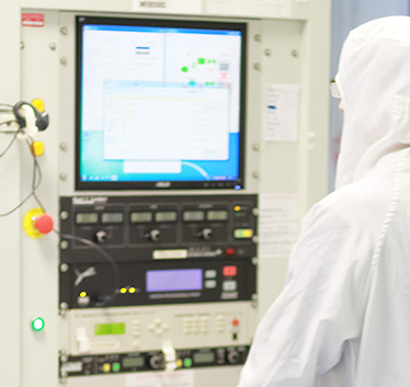
Software, controllers and wafer positioners work together to carefully align wafers for testing, inspection and cutting.
In addition to a wide range of commercial off-the-shelf stages, piezosystem jena has developed stages specifically for wafer positioning. These include the PZ 250 CAP WL z-positioner and the 3-axis TRITOR 320. Customized piezo components as an OEM for semiconductor equipment is always an option for discussion.
FAQ
晶圓定位為什麼需要次奈米解析度?
目前的半導體技術藍圖已把特徵尺寸縮小到個位數奈米,用來製造這些特徵的定位系統也必須具備次奈米等級的解析度。壓電平台可依對位標記或操作人員的指令,以次奈米步距即時調整晶圓位置。
壓電平台能在真空環境裡用嗎?
可以,平台可用於真空或超高真空(UHV)環境,這是晶圓製造流程的必要條件。此外固態設計沒有機械磨耗,可確保長期穩定的使用壽命。
有沒有專為晶圓定位開發的型號?
有。除了完整的標準品平台系列,另有 PZ 250 CAP WL Z 軸定位器與三軸 TRITOR 320 是專為晶圓定位設計的,也可依半導體設備 OEM 的需求討論客製方案。